
 Edit: Judging by responses to this question, my original question must be poorly phrased. I understand the reasons behind the choice of frequency for the system clock to ensure the circuit is stable on the tick of the clock. The responses from @Ran G. and @slebetman emphasize the “contractual” side of things. My question is really about why the contract holds. In retrospect, what I was getting at is the trivial fact that measuring instruments (system clock) must be selected based on the degree of precision required — in a typical case discussed here, for our human sluggish attention span. To illustrate, here’s a graph of the clock pulse against data-in and Qa output for a DFF.
 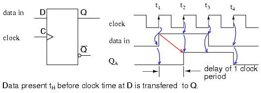 Say, in the 2nd clock cycle, Captain Marvel sends a pulse on the data-in line and — oblivious to the clock period — expects to read it off immediately (mid-phase). With his lightning speed, there’s no way he can make sense of the output of this circuit because the clock cycle is geological time to him. Billy Watson, on the other hand, can read it just fine. Neither Captain M. nor Billy W. is synchronized with the system clock. Not in the sense that the gate circuitry is. But for Billy’s experience of time, the clock’s time scale is sufficiently precise.
Asked By : Maksim Yegorov
Answered By : slebetman
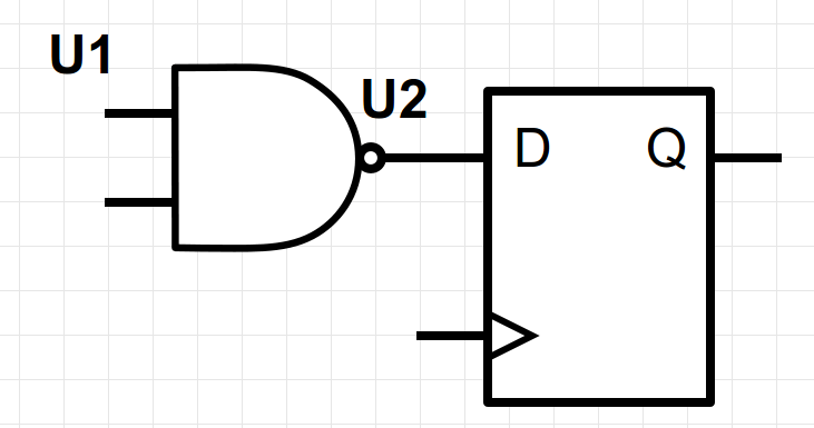
The clock period is set such that the other circuitry (NAND gate in my case) has the time to stabilize during the cycle. This is the contract. But how is it achieved?
Perhaps is overthinking it. It is never achieved. Rather, it is specified. Basically you read the user manual (or in engineering it’s usually the data sheet). If the user manual says the maximum clock is 100MHz then you don’t supply it with a 200MHz clock. That’s the basic mechanism of how it’s “achieved”. So, I can already see the next question forming: How do the designers know to specify 100MHz? It can’t be arbitrary can it? The basic way it’s done is to calculate the timing of all propagation. Say you have this circuit:
output = A && (B || C || (D && E))
Lets say all OR and AND gates have the same propagation time: 1ns. Lets also re-arrange the circuit above to make things clearer:
A / output = && B D / / || && / || E C
So, in the above circuit, the longest path to output is the input from D and E. It passes through four gates (assuming gates can only have two inputs, you can do three levels if you use a three input OR gate). Since each gate takes 1ns to stabilize, the circuit above can be sampled at a rate of every 4ns or 250MHz. The calculations above are simplified of course. It assumes wires have zero propagation time and also assume that inputs are simultaneous. Real-world CAD software can calculate propagation time of wires/traces and can even lengthen traces if necessary to ensure signals arrive at the same time. As for the simultaneity of the inputs, that’s the user’s (the engineer using your component) problem. If the outputs from his circuit take time to stabilize before going in to your circuit he has to take that into account and use a slower clock to allow the signals to stabilize. There is also the dirty way to do the above calculations: overclocking. You keep increasing the clock frequency to your system until it fails then back off a bit until it works again then back off a bit more to allow for some overhead. There’s also a third question and it is part of the assumption of almost every digital designer: When we clock, how are we SURE the inputs have stabilized? We’ve only accounted for the outputs of our gates, not the inputs to them? The answer is that inputs to our circuit comes form another circuit in our system. They synchronize by using the same clock. Since they were clocked at the end of the previous clock cycle, we assume they’re stable at the beginning of this clock cycle. Which is why we only consider the propagation of the gates as the limiting factor for the stability of signals. All non-internal signals or all signals that don’t share our clock must be sampled. That’s part of the reason that external signals can never be as fast as our internal clock – it’s to allow for them to be stable in a register somewhere before signaling to the internal circuits that they’re ready to enter our system. So in general, in terms of signal stability, we assume noise only exists between clock pulses and all the signals in our entire system should stabilize before the next clock pulse. That effectively defines our maximum clock rate.
Best Answer from StackOverflow
Question Source : http://cs.stackexchange.com/questions/48564 Ask a Question Download Related Notes/Documents
